Overview
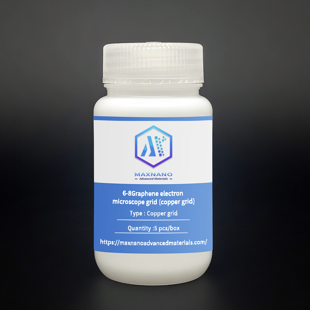
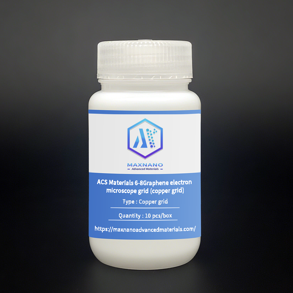
This product consists of 6-8 layer graphene synthesized through chemical vapor deposition (CVD) and transferred onto 2000-mesh copper TEM grids. Utilizing copper’s surface-catalyzed growth mechanism, this multi-layer graphene offers enhanced electronic properties while maintaining excellent structural integrity. Specifically designed for electron microscopy applications, it provides researchers with a reliable sample for detailed nanoscale investigation of thicker graphene systems.
Specifications
-
Substrate: 2000-mesh Copper TEM Grid
-
Graphene Layers: 6-8 layers
-
Growth Method: Catalytic CVD on copper substrate
-
Transfer Process: PMMA-assisted wet transfer
Key Features
-
Enhanced Electronic Properties: Multi-layer structure provides distinctive electronic characteristics suitable for comparative studies
-
High Crystallinity: Maintains graphene’s hexagonal lattice structure across multiple layers
-
Electron Transparency: Optimized thickness allows for effective TEM imaging while preserving structural details
-
Mechanical Resilience: Withstands electron beam exposure during prolonged microscopy sessions
-
Chemical Compatibility: May be treated with dilute acid to reduce catalyst residues if needed
Note
Applications
-
TEM/SEM Analysis: Structural characterization of multi-layer graphene systems
-
Comparative Studies: Investigation of layer-dependent properties in graphene materials
-
Electronic Research: Study of charge transport mechanisms in multi-layer configurations
-
Material Science: Support membrane for nanoparticle imaging and composite material analysis
-
Educational Demonstrations: High-quality sample for microscopy training and research
Contact Information
For detailed product specifications and ordering:
Email: sales@maxnanotech.com

Reviews
There are no reviews yet.