Overview
This product features high-quality CVD graphene transferred onto silicon nitride TEM grids, specifically designed for advanced microscopy and nanomaterial research. Utilizing catalytic chemical vapor deposition on metal substrates followed by a PMMA-assisted transfer process, these samples provide excellent electron transparency and mechanical stability for high-resolution TEM characterization. The silicon nitride substrate offers superior thermal and mechanical properties compared to conventional carbon-based TEM grids, making it ideal for demanding imaging applications.
Specifications
-
Substrate: Silicon Nitride Membrane
-
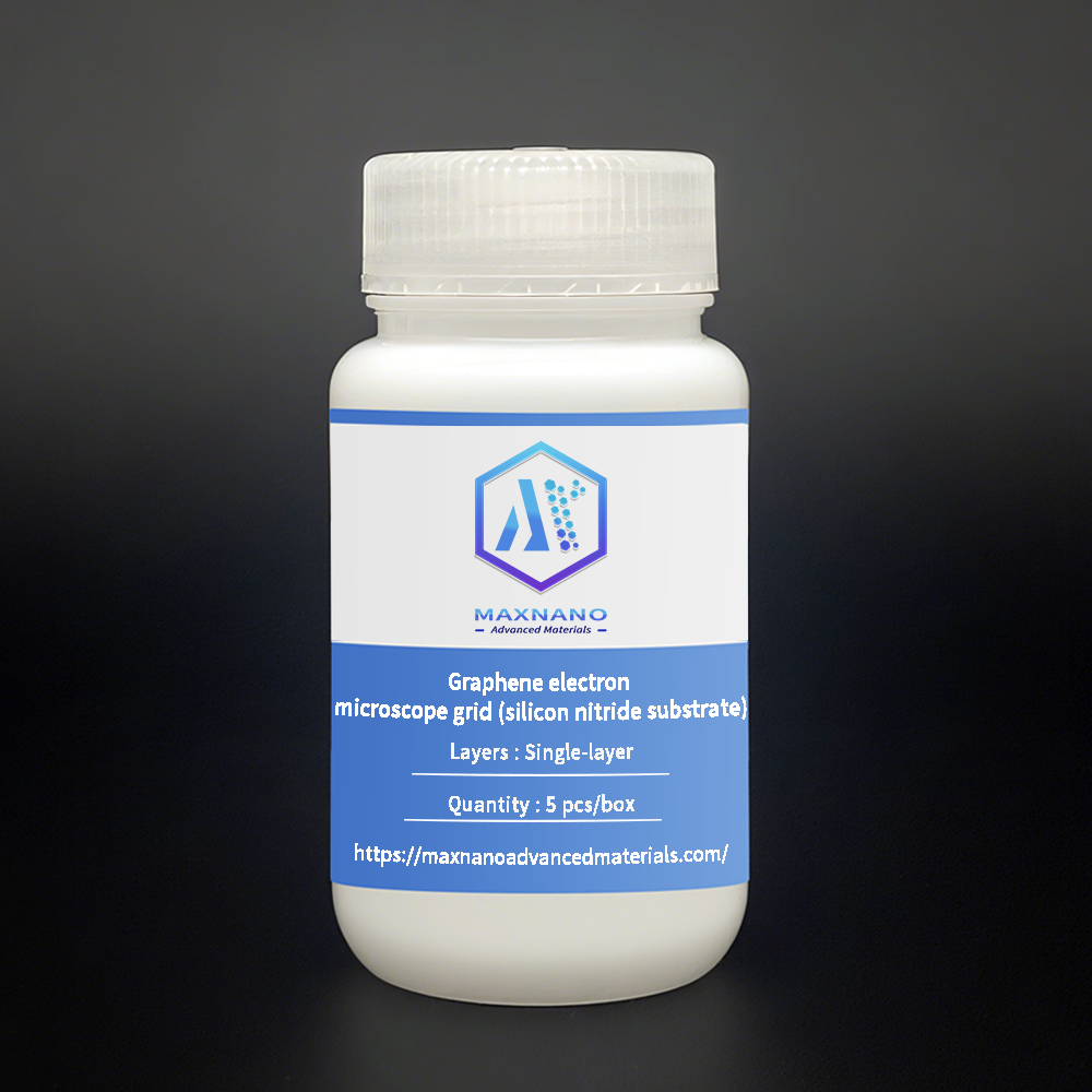
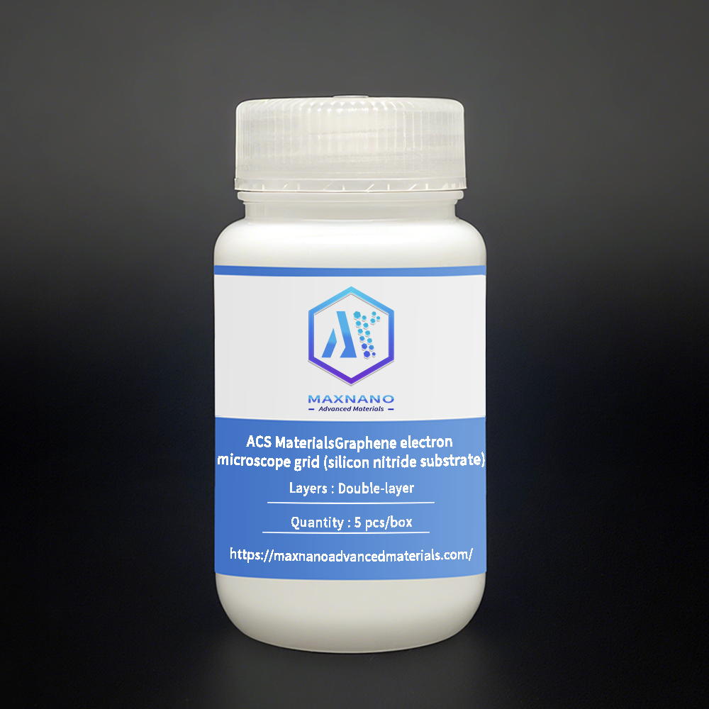
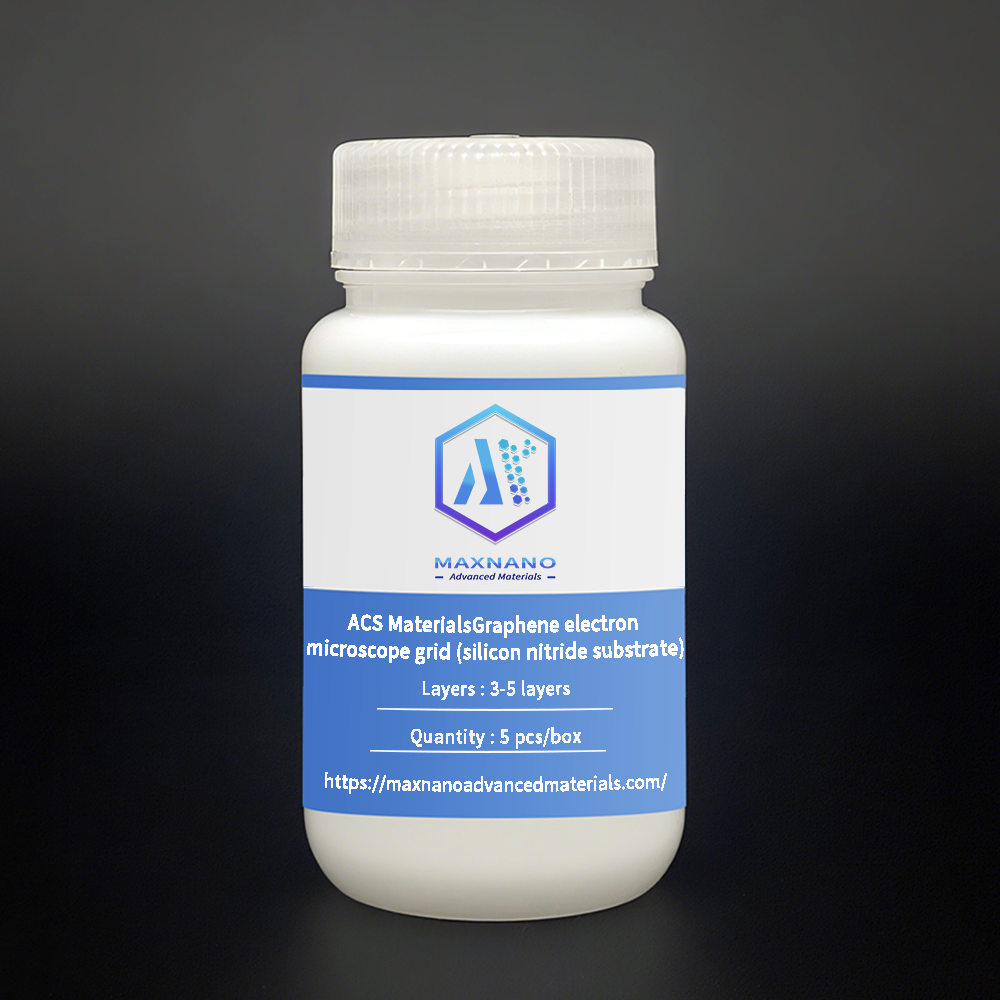
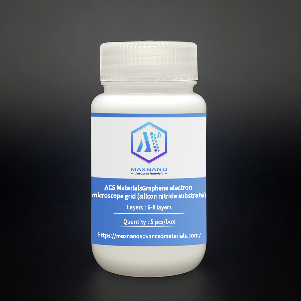
Available Layers: Monolayer, Bilayer, 3-5 Layers, 6-8 Layers
-
Grid Type: Standard TEM Grid Format
Key Features
-
Superior Electron Transparency: Silicon nitride substrate provides excellent imaging quality with low background noise
-
High Crystallinity: Maintains graphene’s characteristic hexagonal lattice structure
-
Thermal Stability: Withstands higher beam currents and longer exposure times than conventional grids
-
Mechanical Robustness: Silicon nitride membrane offers improved durability during handling and imaging
-
Customizable Layer Number: Available in various layer configurations for comparative studies
Applications
-
High-Resolution TEM: Atomic-scale imaging of graphene defects and grain boundaries
-
In Situ Studies: Suitable for heating, biasing, and environmental TEM experiments
-
Nanoparticle Research: Ideal support for nanoparticle dispersion and catalysis studies
-
Electronic Property Characterization: Layer-dependent electronic structure investigation
-
Educational Use: Premium samples for advanced microscopy training and demonstration
Note
-
Some catalyst residues may appear as dark spots under TEM – this is normal and can potentially be reduced with dilute acid treatment
-
Samples are packaged in standard TEM grid holders for safe storage and handling
Contact Information
For technical specifications and custom layer requests:
Email: sales@maxnanotech.com


Reviews
There are no reviews yet.