Overview
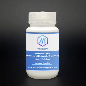
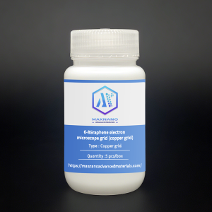
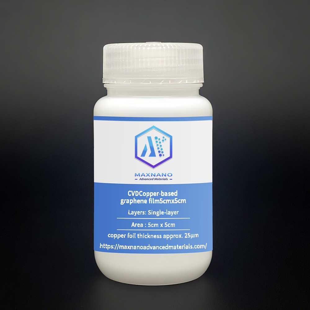
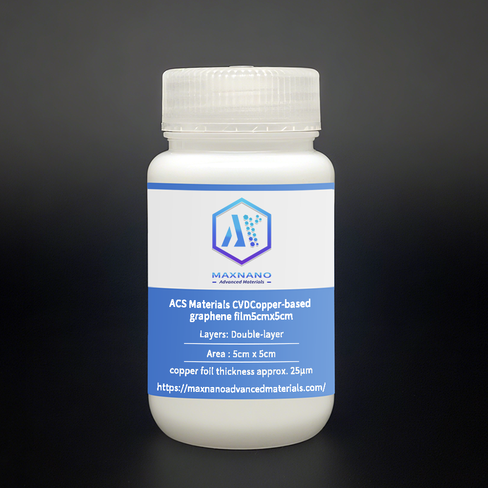
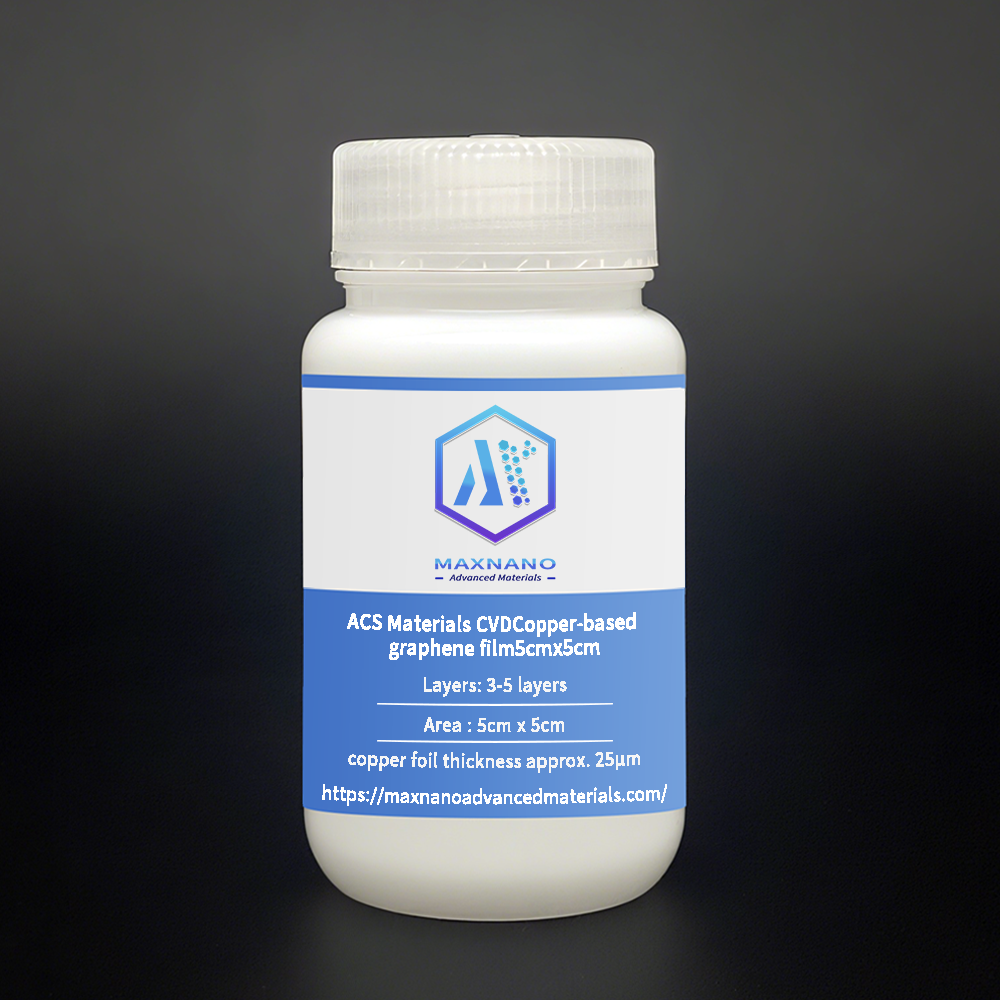
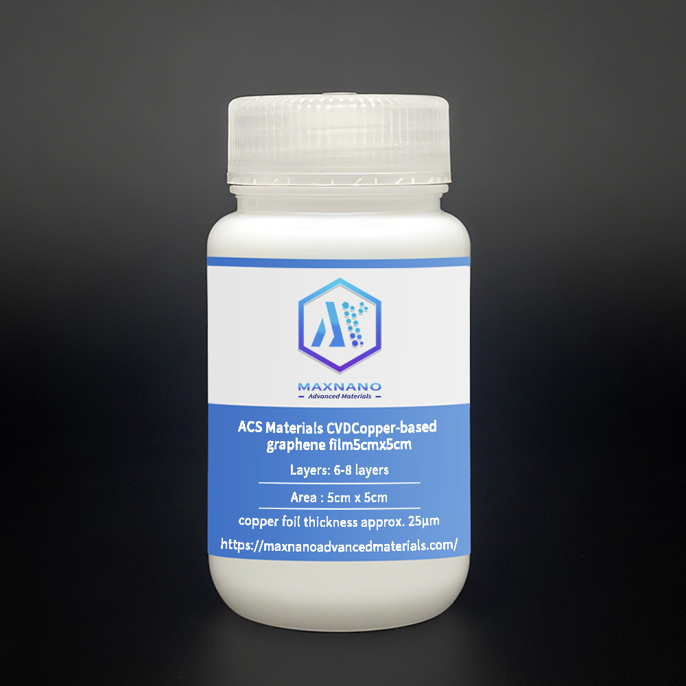
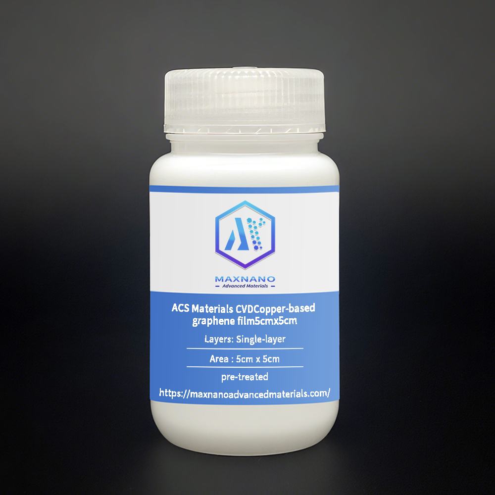
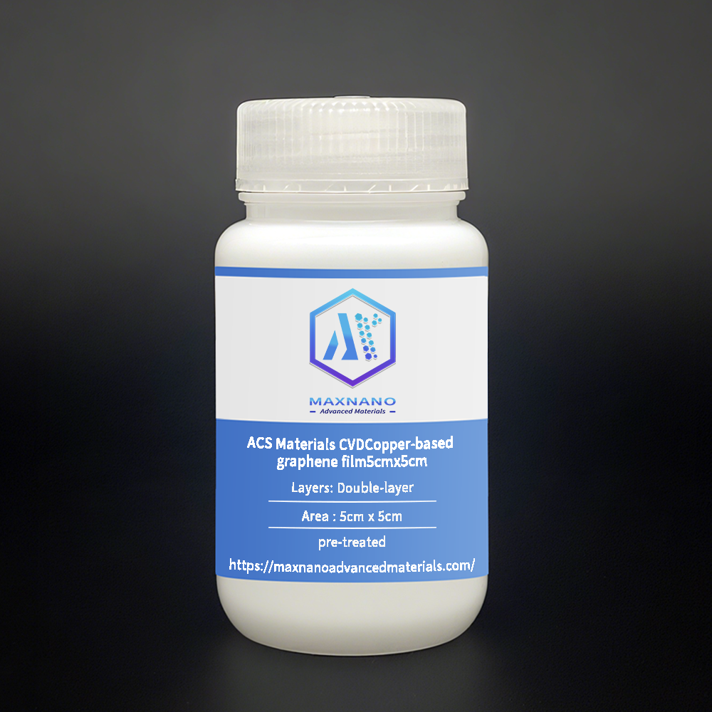
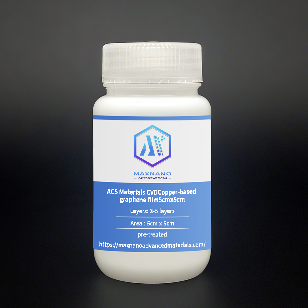
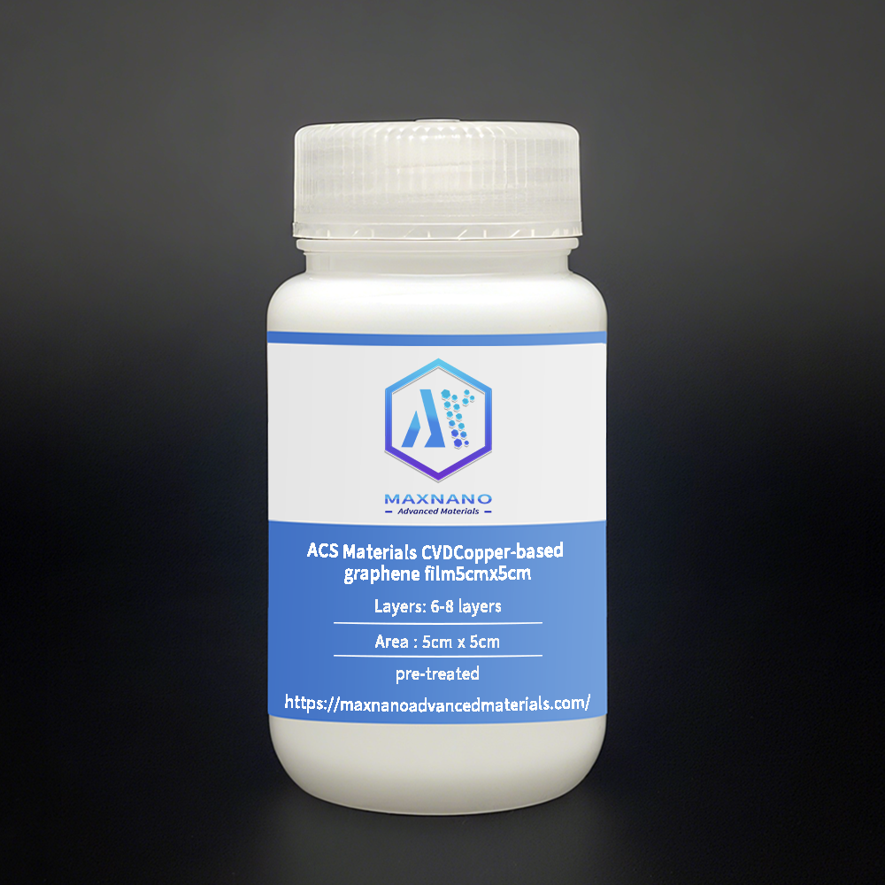
CVD graphene synthesis relies on three essential elements: substrate selection, carbon precursor gases, and optimized growth conditions. Copper foil serves as an ideal substrate for graphene growth due to its catalytic surface behavior and self-limiting growth mechanism, which promotes the formation of large-area, high-quality monolayer graphene. This product provides graphene directly on a 5 cm × 5 cm copper foil, ready for transfer to desired substrates or direct use in certain applications.
Specifications
-
Substrate: Copper foil
-
Copper Thickness: ~25 µm
-
Graphene Area: 5 cm × 5 cm
-
Available Layers: Monolayer, Bilayer, 3–5 Layers, 6–8 Layers
Key Features
-
High Crystallinity and Uniform Coverage: Ensures consistent electronic and mechanical performance
-
Excellent Electrical Properties: High carrier mobility and low sheet resistance
-
High Optical Transparency: Suitable for optoelectronic applications
-
Outstanding Mechanical Flexibility and Strength: Ideal for flexible electronics and composites
-
High Chemical Stability: Performs reliably under ambient conditions
Applications
-
Electronic Devices: Field-effect transistors, integrated circuits, and flexible electronics
-
Optoelectronics: Transparent conductive films, touch screens, and light-emitting devices
-
Sensors: Highly sensitive chemical and biological detection platforms
-
Energy Systems: Electrodes for solar cells, supercapacitors, and batteries
-
Advanced Composites: Used as a functional interface to enhance material properties
Note
Customers may specify pretreatment requirements:
-
PMMA spin-coating on the graphene side for protection
-
Back-side copper etching for partial or full transfer
-
Default service includes PMMA coating, etching, and transfer to a silicon oxide substrate, accompanied by Raman quality analysis.
Contact Information
For product inquiries, layer specifications, or custom pretreatment services, please contact:
Email: sales@maxnanotech.com


Reviews
There are no reviews yet.