Email

beikeheq@gmail.com

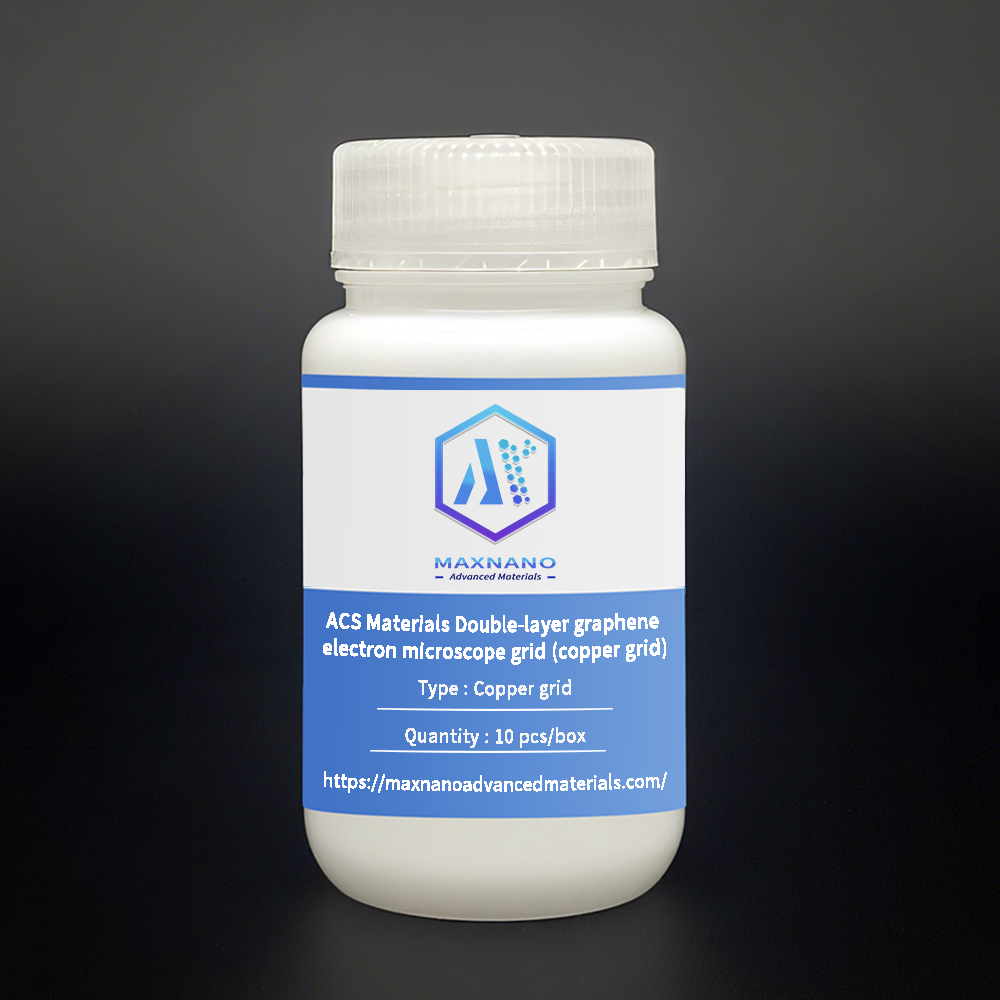
Double-layer graphene electron microscope grid (copper grid)

Price range: $510.42 through $937.50

Precisely controlled bilayer CVD graphene on ultra-fine 2000-mesh copper TEM grids. Enables atomic-resolution imaging of Moiré patterns and interlayer interactions, ideal for twist angle studies and quantum phenomena research.

Grid Type: 2000-mesh Copper
Graphene Layers: Bilayer
Transfer Method: PMMA-assisted
Contact:  sales@maxnanotech.com

Important Notes

  •  No Refunds or Exchanges: All sales are final. MAXNANO does not provide return, exchange, or refund services under any circumstances.
  • Customs and Import Obligations: Clearance procedures, import duties, taxes, and related costs are solely the responsibility of the recipient/importer. MAXNANO shall not be held liable for delays, rejections, or any additional expenses incurred during customs processes. Such issues shall not constitute grounds for order cancellation or refund.
  • Order Cancellation: Orders cannot be revoked once submitted. No refunds will be issued for cancelled or undelivered orders.
  • Indemnification: The purchaser agrees to bear all claims, losses, legal liabilities, and expenses arising from the use of products and services, and shall hold MAXNANO, its affiliates, and personnel harmless from such obligations.
  • Terms and Conditions: All orders and business interactions are subject to MAXNANO’s standard Terms and Agreements.

Inquiry Now

Overview
This product features precisely controlled bilayer CVD graphene transferred onto ultra-fine 2000-mesh copper TEM grids. Utilizing optimized chemical vapor deposition processes on copper substrates, these samples provide exceptional quality for studying the unique electronic and structural properties of bilayer graphene systems. The high-density 2000-mesh grid offers superior support for atomic-resolution characterization while maintaining excellent electron transparency.

Specifications

  • Support Grid: 2000-mesh Copper

  • Graphene Layers: Bilayer

  • Growth Substrate: Copper foil

  • Transfer Method: PMMA-assisted process

Key Features

  • Layer Precision: Controlled bilayer structure with consistent interlayer spacing

  • Ultra-Fine Support: 2000-mesh grid enables high-resolution imaging

  • Excellent Crystallinity: Maintains graphene’s superior electronic properties

  • Research Ready: Pre-mounted on TEM grids for immediate use

  • Stacking Analysis: Ideal for investigating twist angles and interlayer interactions

Applications

  • Moiré Pattern Studies: Investigation of bilayer graphene’s unique electronic properties

  • Comparative Research: Direct comparison with monolayer and few-layer structures

  • Quantum Phenomena: Study of layer-dependent quantum transport properties

  • Advanced Materials: Support for nanoparticle and hybrid material research

  • Educational Excellence: Premium samples for nanotechnology education and research

Note

  • Some catalyst residues may appear as dark spots under TEM – normal byproduct of CVD process

  • Optional dilute acid treatment available for reduced residue visibility

  • Store in dry conditions at room temperature

Contact Information
For technical specifications and ordering:
Email: sales@maxnanotech.com

Weight 100 g
Dimensions 30 × 20 mm
Specification

Copper grid, 5 pcs/box, 5 pcs, Copper grid, 10 pcs/box, 10 pcs

Reviews

There are no reviews yet.

Be the first to review “Double-layer graphene electron microscope grid (copper grid)”

Your email address will not be published. Required fields are marked *

Scroll to Top