Email

beikeheq@gmail.com

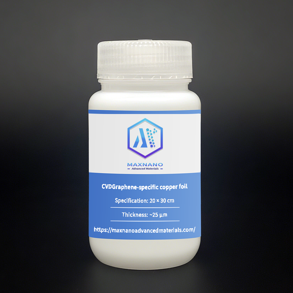
CVDGraphene-specific copper foil

$104.17

20 × 30 cm, 25 μm thick, >99.9% purity. Ultra-smooth surface (<5 nm RMS), large grain size (>100 μm after annealing). Optimized for high-quality, low-defect monolayer graphene growth.

  • Pre-annealed at 1000°C for reduced nucleation

  • Applications: R&D and industrial graphene production

  • Ensures high carrier mobility and reproducible results

Email: Sales@maxnanotech.com

Important Notes

  •  No Refunds or Exchanges: All sales are final. MAXNANO does not provide return, exchange, or refund services under any circumstances.
  • Customs and Import Obligations: Clearance procedures, import duties, taxes, and related costs are solely the responsibility of the recipient/importer. MAXNANO shall not be held liable for delays, rejections, or any additional expenses incurred during customs processes. Such issues shall not constitute grounds for order cancellation or refund.
  • Order Cancellation: Orders cannot be revoked once submitted. No refunds will be issued for cancelled or undelivered orders.
  • Indemnification: The purchaser agrees to bear all claims, losses, legal liabilities, and expenses arising from the use of products and services, and shall hold MAXNANO, its affiliates, and personnel harmless from such obligations.
  • Terms and Conditions: All orders and business interactions are subject to MAXNANO’s standard Terms and Agreements.

Inquiry Now

Product Overview
We supply specialized copper foil optimized for chemical vapor deposition (CVD) graphene growth. Our foil undergoes precise annealing and surface treatment to provide an ideal substrate for producing high-quality, large-area graphene films with excellent crystalline structure and electrical properties.

Specifications

  • Dimensions: 20 × 30 cm

  • Thickness: ~25 μm

  • Purity: >99.9 wt%

  • Surface Roughness: <5 nm RMS

  • Grain Size: >100 μm after annealing

Key Properties

  • High Purity: Minimizes impurity interference during graphene growth

  • Excellent Surface Flatness: Provides uniform substrate for consistent graphene formation

  • Optimized Grain Structure: Reduced grain boundaries for lower nucleation density

  • Thermal Stability: Maintains structural integrity at high temperatures

  • Surface Quality: Ultra-smooth surface for continuous graphene films

Pre-Treatment Process

  • Annealing at 1000°C for 30 minutes

  • Grain growth and boundary reduction

  • Surface oxidation removal

  • Contamination-free handling

Product Features

  • Specifically designed for CVD graphene synthesis

  • Consistent surface quality across entire foil

  • Reduced graphene nucleation defects

  • Enhanced graphene carrier mobility

  • Reproducible growth results

Primary Application

  • CVD Graphene Growth: Ideal substrate for high-quality monolayer graphene production

  • Research & Development: Reproducible platform for graphene studies

  • Industrial Production: Scalable substrate for commercial graphene manufacturing

Technical Advantages

  • Lower graphene nucleation density

  • Improved graphene crystal quality

  • Enhanced electrical properties

  • Larger single-crystal graphene domains

  • Better batch-to-batch consistency

Quality Assurance

  • Purity verification through composition analysis

  • Surface roughness measurement

  • Grain size characterization

  • Contamination testing

  • Performance validation in graphene growth

Contact Information
For technical specifications and ordering:
Email: Sales@maxnanotech.com

Weight 100 g
Dimensions 30 × 20 × 20 mm
Specification

Dimension: 20 cm × 30 cm; Thickness: ~25 μm

Reviews

There are no reviews yet.

Be the first to review “CVDGraphene-specific copper foil”

Your email address will not be published. Required fields are marked *

Scroll to Top