
How Nanoimprint Lithography Is Empowering AR and Biochips
2025 marks the 30th anniversary of Nanoimprint Lithography (NIL). First developed by Professor Stephen Chou’s team in 1995, NIL has become a key method for producing deep-nanoscale patterns. Over time, it has grown from a laboratory technique into an industrial solution. In some fields, it has even become a practical and cost-effective alternative to Extreme Ultraviolet (EUV) lithography.
30 Years of Progress: From Lab to Fab

What is NIL?
Nanoimprint Lithography forms nanoscale patterns through mechanical molding rather than optical exposure. Therefore, it is not limited by optical diffraction, which allows NIL to achieve high resolution at lower cost.
Over the past three decades, NIL has expanded into several formats:
Thermal NIL
UV-based NIL
Roll-to-roll continuous NIL
In addition, major equipment advances have pushed NIL toward industrial manufacturing. For example, in 2023, Canon introduced a semiconductor-grade NIL platform capable of 26 nm half-pitch resolution, with potential for 14 nm. As a result, NIL is now a competitive solution for flash memory, MEMS devices, and sensor fabrication.
A Key Breakthrough: Large-Area, High-Uniformity Imprinting
Recent research has focused on improving large-area imprint quality.
Traditionally, NIL struggled with pattern uniformity and defect rates, especially on large wafers. However, new improvements in template design, resist chemistry, and pressure control have expanded imprint areas to 12 inches and beyond, while keeping defects within industrial standards.
This breakthrough is essential for:
AR optical waveguides
Planar optics
High-density biochips
According to long-term research published in Tribology International and other nanofabrication journals, nanoimprint lithography continues to demonstrate strong scalability for large-area nanostructuring. For additional background on how NIL functions as a high-resolution, high-throughput, and scalable nanofabrication technique, see the Nanoimprint Lithography overview on Wikipedia: https://en.wikipedia.org/wiki/Nanoimprint_lithography
Empowering Cutting-Edge Applications: AR and Biochips
1. AR Glasses: The Optical Core
The core display element in AR glasses depends on nanoscale diffraction gratings that guide and project images. EUV lithography is expensive and inefficient for large substrates. Therefore, NIL offers a lower-cost and high-throughput alternative for manufacturing AR waveguide components.
2. Biochips for Genetic Sequencing
In next-generation sequencing, NIL enables the fabrication of high-density microfluidic and molecular reaction sites. As a result, sequencing becomes faster, more precise, and easier to scale, greatly benefiting biomedical diagnostics and research.
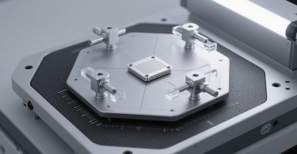
The Future: Complementarity and Innovation
NIL is unlikely to replace EUV entirely.
However, it will continue to expand in fields that require very high resolution but also demand lower cost and higher efficiency.
Future progress will likely center on:
New imprint resin materials
Hybrid processing combining NIL with EUV or optical lithography
Smarter process monitoring and control
In summary, nanoimprint lithography is transitioning from a specialized laboratory technique into a practical industrial manufacturing technology. As NIL continues to enable scalable nanostructuring for AR optics, biochips, and advanced microdevices, industry-driven platforms that focus on advanced nanomaterials and fabrication technologies are becoming increasingly important. To learn more about our background and long-term focus in this field, visit our About Us page at MaxNano Advanced Materials:
https://maxnanoadvancedmaterials.com/about-us/
NIL Process Advantages Compared with Conventional Lithography
From a manufacturing perspective, nanoimprint lithography offers several advantages over traditional optical lithography methods. Unlike projection-based exposure systems, NIL relies on direct physical contact between the template and the resist layer. This fundamental difference allows NIL to bypass optical diffraction limits entirely.
As a result, NIL can achieve sub-20 nm feature sizes without the need for complex optical systems or extreme ultraviolet light sources. In addition, the overall tool cost and energy consumption are significantly lower compared with EUV lithography, making NIL especially attractive for cost-sensitive applications and large-area patterning.
In practical production environments, NIL also demonstrates excellent pattern fidelity and repeatability when combined with optimized resist formulations and anti-sticking surface treatments. These improvements have greatly reduced defect density, one of the main barriers that previously limited large-scale adoption.
Engineering Challenges and Ongoing Optimization
Despite its advantages, nanoimprint lithography still faces engineering challenges that are actively being addressed by both academic and industrial researchers. One key issue is template durability. Because NIL templates come into direct contact with the resist, mechanical wear and contamination can affect long-term process stability.
To mitigate this, advanced hard coatings and surface functionalization techniques have been introduced to extend template lifetime. At the same time, real-time process monitoring systems are being integrated into NIL tools to detect pressure variations, alignment errors, and defect formation during imprinting.
Another challenge involves overlay accuracy, especially when NIL is used in multi-layer device fabrication. Hybrid process flows—combining NIL with optical lithography for critical alignment steps—are emerging as a practical solution in semiconductor and biochip manufacturing.
Expanding Impact on AR, Biochips, and Emerging Devices
The ability of nanoimprint lithography to deliver high-resolution patterns over large areas is particularly valuable for augmented reality optics and bio-integrated devices. In AR waveguides, nanoscale gratings must be fabricated with extreme uniformity to ensure optical efficiency and image clarity. NIL provides a scalable way to manufacture these structures without the prohibitive cost of EUV systems.
Similarly, in biochip and lab-on-a-chip technologies, NIL enables dense arrays of micro- and nanoscale features that control fluid flow, molecular binding, and signal detection. These capabilities are accelerating advances in genetic sequencing, point-of-care diagnostics, and personalized medicine.
Beyond AR and biochips, NIL is also gaining traction in metasurfaces, flexible electronics, and next-generation sensors, where precise nanoscale patterning directly translates into device performance.
Industry Outlook and Future Development
Looking ahead, nanoimprint lithography is expected to play a complementary role alongside EUV and advanced optical lithography rather than fully replacing them. Its strength lies in applications that require ultra-high resolution, large-area coverage, and cost efficiency.
Future innovation will likely focus on new imprint materials, automated defect control, and deeper integration with existing semiconductor process flows. As these challenges continue to be addressed, NIL will further establish itself as a key enabling technology for next-generation micro- and nanoscale manufacturing.